- 您现在的位置:买卖IC网 > Sheet目录475 > MC33493MOD868EV (Freescale Semiconductor)BOARD EVAL MC33493 TANGO
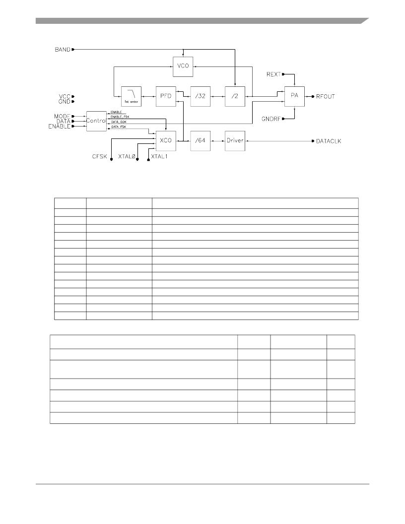
Figure 1. Simplified Block Diagram
Table 1. Pin Function Description
Pin
1
2
3
4
5
6
7
8
9
10
11
12
13
14
Name
DATACLK
DATA
BAND
GND
XTAL1
XTAL0
REXT
CFSK
VCC
RFOUT
GNDRF
VCC
ENABLE
MODE
Description
Clock output to the microcontroller
Data input
Frequency band selection
Ground
Reference oscillator input
Reference oscillator output
Power amplifier output current setting input
FSK switch output
Power supply
Power amplifier output
Power amplifier ground
Power supply
Enable input
Modulation type selection input
Table 2. Absolute Maximum Ratings
Supply voltage
Voltage allowed on each pin
Parameter
Symbol
V CC
Value
V GND – 0.3 to 3.7
V GND – 0.3
Unit
V
V
to V CC + 0.3
ESD MM voltage capability on each pin (note 2)
ESD HBM voltage capability on each pin 1 (note 1)
2
± 2000
± 150
V
V
Storage temperature
Junction temperature
1
Human Body model, AEC-Q100-002 Rev. C.
2
Machine Model, AEC-Q100-003 Rev. E.
Ts
Tj
–65 to +150
+150
° C
° C
PLL Tuned UHF Transmitter for Data Transfer Applications, Rev. 1.7
Freescale Semiconductor
3
发布紧急采购,3分钟左右您将得到回复。
相关PDF资料
MC33591MOD315EV
BOARD EVAL MC33493 TANGO3 RF
MC33593MOD868EV
BOARD EVAL MC33593 ROMEO2 RF
MC33690DWER2
IC STAND ALONE TAG READER 20SOIC
MC44CC375AVEFEVK
CCEVK NEJA EVAL KIT
MCH3374-TL-E
MOSFET P-CH 12V 3A MCPH3
MCH3375-TL-H
MOSFET P-CH 1.6A 30V MCPH3
MCH3377-TL-E
MOSFET P-CH 20V 3A MCPH3
MCH3377-TL-H
MOSFET P-CH 3A 20V MCPH3
相关代理商/技术参数
MC3350-041-91
制造商:SPC Multicomp 功能描述:ROCKER SWITCH DPDT CTR OFF 制造商:SPC Multicomp 功能描述:ROCKER SWITCH, DPDT, CTR OFF 制造商:SPC Multicomp 功能描述:SWITCH, ROCKER, DPDT, 15A, 250V, BLACK; Contact Configuration:DPDT; Switch Operation:On-Off-On; Contact Current Max:10A; Contact Voltage AC Nom:250V; Contact Voltage DC Nom:250V; Switch Mounting:Panel; Actuator / Cap Color:Black ;RoHS Compliant: Yes
MC3350-041-91
制造商:SPC Multicomp 功能描述:SWITCH ROCKER DPDT CTR OFF
MC33501SNT1
功能描述:运算放大器 - 运放 1-7V Single Rail to RoHS:否 制造商:STMicroelectronics 通道数量:4 共模抑制比(最小值):63 dB 输入补偿电压:1 mV 输入偏流(最大值):10 pA 工作电源电压:2.7 V to 5.5 V 安装风格:SMD/SMT 封装 / 箱体:QFN-16 转换速度:0.89 V/us 关闭:No 输出电流:55 mA 最大工作温度:+ 125 C 封装:Reel
MC33501SNT1G
功能描述:运算放大器 - 运放 1-7V Single Rail to Rail -40 to 105 Cel RoHS:否 制造商:STMicroelectronics 通道数量:4 共模抑制比(最小值):63 dB 输入补偿电压:1 mV 输入偏流(最大值):10 pA 工作电源电压:2.7 V to 5.5 V 安装风格:SMD/SMT 封装 / 箱体:QFN-16 转换速度:0.89 V/us 关闭:No 输出电流:55 mA 最大工作温度:+ 125 C 封装:Reel
MC33501SNT1G
制造商:ON Semiconductor 功能描述:OP AMP SINGLE R/R SMD SOT23-5
MC33501SNT1GH
制造商:Rochester Electronics LLC 功能描述: 制造商:ON Semiconductor 功能描述:
MC33502D
功能描述:运算放大器 - 运放 1-7V Dual Rail to RoHS:否 制造商:STMicroelectronics 通道数量:4 共模抑制比(最小值):63 dB 输入补偿电压:1 mV 输入偏流(最大值):10 pA 工作电源电压:2.7 V to 5.5 V 安装风格:SMD/SMT 封装 / 箱体:QFN-16 转换速度:0.89 V/us 关闭:No 输出电流:55 mA 最大工作温度:+ 125 C 封装:Reel
MC33502DG
功能描述:运算放大器 - 运放 1-7V Dual Rail to Rail -40 to 105 Cel RoHS:否 制造商:STMicroelectronics 通道数量:4 共模抑制比(最小值):63 dB 输入补偿电压:1 mV 输入偏流(最大值):10 pA 工作电源电压:2.7 V to 5.5 V 安装风格:SMD/SMT 封装 / 箱体:QFN-16 转换速度:0.89 V/us 关闭:No 输出电流:55 mA 最大工作温度:+ 125 C 封装:Reel
